Links to external sources may no longer work as intended. The content may not represent the latest thinking in this area or the Society’s current position on the topic.
New horizons in nanophotonics
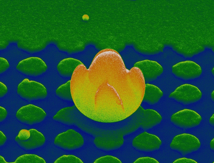
Theo Murphy scientific meeting organised by Professor Yuri Kivshar, Professor Nikolay Zheludev, Professor Ortwin Hess and Professor Bill Barnes.
This meeting will bring together leading researchers from different areas of nanoscale physics to explore the confluence of subwavelength photonics, metamaterials, graphene physics, and nonlinear optics. Whilst a number of breakthroughs can be already anticipated, such as energy saving metadevices for optical technologies, the primary objective of this meeting is to catalyse the creation of new exciting areas in nanophotonics.
Speaker biographies, abstracts, and recorded audio of the presentations is available below. Papers from the meeting will be published in a future issue of Philosophical Transactions A.
Enquiries: Contact the events team
Organisers
Schedule
Chair
Professor Yuri Kivshar, Australian National University, Australia

Professor Yuri Kivshar, Australian National University, Australia
Yuri S. Kivshar received a PhD degree in theoretical physics in 1984 from the Institute for Low Temperature Physics and Engineering (Kharkov, Ukraine). From 1988 to 1993 he worked at different research centers in USA, France, Spain, and Germany, and in 1993 he moved to Australia where later he established Nonlinear Physics Center at the Australian National University being currently Head of the Center and Distinguished Professor. His research interests include nonlinear photonics, optical solitons, nanophotonics, and metamaterials. He is Fellow of the Australian Academy of Science, the Optical Society of America, the American Physical Society, the Institute of Physics (UK), as well as Deputy Director of the Center of Excellence for Ultrahigh-bandwidth Devices for Optical Systems CUDOS (Australia) and Research Director of Metamaterial Laboratory (Russia). He received many prestigious awards including the Lyle Medal (Australia), the State Prize in Science and Technology (Ukraine), and the Harrie Massey Medal of the Institute of Physics (UK).
| 09:05 - 09:30 |
Sculpting waves for desired functionalities
Owing to the recent advances in nanoscience, nanotechnology, and materials science and engineering, it has become possible to engineer materials and platforms with unprecedented features and characteristics that allow unconventional control and manipulation of waves and fields at subwavelength scales. In my group, we are exploring electromagnetic and optical wave interaction in platforms with extreme scenarios, such as materials with near-zero parameters (e.g., near-zero permittivity and near-zero permeability), and with extreme features such as very high phase velocity, very low group velocity, one-way vortices at the nanoscale, giant anisotropy and nonlinearity, “near-zero photonics”, nanoscale computation with optical nanocircuits, and more. Such “extreme control” on fields and waves provides us with exciting features and functionalities for wave-based paradigms such as optics, acoustics, and thermodynamics. In this presentation, I will present most recent results from some of our ongoing efforts in these areas, and will forecast some future directions and possibilities. 
Professor Nader Engheta, University of Pennsylvania, USA

Professor Nader Engheta, University of Pennsylvania, USANader Engheta is the H. Nedwill Ramsey Professor at the University of Pennsylvania in Philadelphia. He received his PhD degree from Caltech. Selected as one of the Scientific American Magazine 50 Leaders in Science and Technology in 2006 for developing the concept of optical lumped nanocircuits, he is a Guggenheim Fellow, an IEEE Third Millennium Medalist, a Fellow of IEEE, APS, OSA, SPIE, and American Association for the Advancement of Science (AAAS), and the recipient of numerous awards for his research including 2014 Balthasar van der Pol Gold Medal from URSI, 2013 Benjamin Franklin Key Award, 2013 Inaugural SINA Award in Engineering, 2012 IEEE Electromagnetics Award, 2008 George H. Heilmeier Award for Excellence in Research, the Fulbright Naples Chair Award, NSF Presidential Young Investigator award, the UPS Foundation Distinguished Educator term Chair, and several teaching awards. He has co-edited the book entitled “Metamaterials: Physics and Engineering Explorations” by Wiley-IEEE Press, 2006. He was the Chair of the Gordon Research Conference on Plasmonics in June 2012. |
|
|---|---|---|
| 09:45 - 10:15 |
Non-Hermitian light matter interactions: exploiting the optical loss
Optical loss is usually undesirable. Recently, judiciously designed balanced gain and loss structures, so called parity-time (PT) symmetric synthetic systems, are explored due to their extraordinary properties. In this talk I will discuss the notion of PT symmetry in optical systems. Especially I will discuss how to achieve nano-scale spectrometer by designing an anti-Hermitian light matter interactions. This will be also useful for spectrum splitting in solar applications. Finally, I will discuss a single mode lasing scheme using PT symmetric periodically modulation in a micro ring lasers. 
Professor Xiang Zhang, University of California at Berkeley, USA

Professor Xiang Zhang, University of California at Berkeley, USAXiang Zhang is the Ernest S. Kuh Chaired Professor at the University of California, Berkeley and Director of Materials Science Division at Lawrence Berkeley National Laboratory (LBNL). He is also the Director of the NSF Nano-scale Science and Engineering Center (SINAM). He is a member of the US National Academy of Engineering (NAE), Academia Sinica and fellow of APS, OSA, AAAS and SPIE. His group’s research in optical metamaterials was selected by Times Magazine as “Top 10 Scientific Discoveries in 2008”. Xiang Zhang was a recipient of the NSF CAREER Award, Rohsenow Lecturer at MIT, William C. Reynolds Lecturer at Stanford University, Fred Kavli Distinguished Lecturer at Materials Research Society (MRS), Dell K. Allen Outstanding Young Engineer Award and ONR Young Investigator Award. In 2014, he was awarded Fitzroy Medal for pioneering contribution in metamaterials and superlens. |
|
| 11:00 - 11:30 |
Nanosystems in ultrafast and superstrong fields: attosecond phenomena
We present our latest results for a new class of phenomena in condensed matter nanooptics when a strong optical field ∼1-3 V/Å changes a solid within optical cycle. Such a pulse drives ampere-scale currents in dielectrics and adiabatically controls their properties, including optical absorption and reflection, extreme UV absorption, and generation of high harmonics in a non-perturbative manner on a 100-as temporal scale. Applied to a metal, such a pulse causes an instantaneous and, potentially, reversible change from the metallic to semimetallic properties. We will also discuss our latest theoretical results on graphene that in a strong ultrashort pulse field exhibits unique behavior. New phenomena are predicted for buckled two-dimensional solids, silicene and germanine. These are fastest phenomena in optics unfolding within half period of light. They offer potential for petahertz-bandwidth signal processing, generation of high harmonics on a nanometer spatial scale, etc. 
Professor Mark Stockman, Georgia State University, USA

Professor Mark Stockman, Georgia State University, USAMark I. Stockman received his PhD and DSc degrees from institutes of the Russian Academy of Sciences. Currently he is Professor of Physics at Georgia State University, Atlanta, GA, USA. He also served as a Distinguished Professor at Ecole Normale Supérieure de Cachan (France) and Ecole Supérieure de Physique and de Chimie Industrielle (Paris, France), and also as a Guest Professor at University of Stuttgart (Germany), Max Plank Institute for Quantum Optics (Garching, Germany), and Ludwig Maximilian University (Munich, Germany). A major direction of his research is theoretical nanoplasmonics, especially theory of ultrafast and nonlinear nanoscale optical phenomena. He is a co-inventor of SPASER (nanoplasmonic laser). He is an author of 160 major research papers and presented many invited and keynote talks at major international conferences. He taught short courses on nanoplasmonics and related topics at major international meetings and scientific institutions in US, Canada, Europe, Asia, and Australia. |
|
| 11:45 - 12:15 |
Cooling and amplification of a vacuum-trapped nanoparticle
I discuss our experiments with optically levitated nanoparticles in ultrahigh vacuum.Using an active parametric feedback scheme we cool the particle’s center-of-mass temperature to T ~ 500μK and reach mean quantum occupation numbers of n ~ 50. I show that mechanical quality factors of Q = 109 can be reached and that damping is dominated by photon recoil heating. The vacuum-trapped nanoparticle forms an ideal model system for studying non-equilibrium processes, nonlinear interactions, and ultrasmall forces. 
Professor Lukas Novotny, ETH Zürich, Switzerland

Professor Lukas Novotny, ETH Zürich, SwitzerlandLukas Novotny is a Professor of Photonics at ETH Zürich since 2012. Before joining ETH, he has been on the faculty of the Institute of Optics at the University of Rochester for 13 years. Novotny's group studies antenna-coupled light-matter interactions for use in photodetection, develops nanoparticle detectors for contamination control, and explores the quantum limit of vacuum-trapped particles. Novotny is author of the textbook 'Principles of Nano-Optics'. He is a Fellow of the Optical Society of America and the American Association for the Advancement of Science.
|
Chair
Professor Nikolay Zheludev, University of Southampton, UK

Professor Nikolay Zheludev, University of Southampton, UK
Professor Nikolay Zheludev’s research interests are in nanophotonics and metamaterials. He directs the Centre for Photonic Metamaterials at Southampton University, UK and Centre for Disruptive Photonic Technologies at Nanyang Technological University, Singapore. He is also founding co-Director of the Photonics Institute at NTU, Singapore and Deputy Director of the Optoelectronics Research Centre at Southampton. His personal awards include the Royal Society Wolfson Merit Award and Senior Research Professorships of the EPSRC and the Leverhulme Trust. In 2015 he was awarded the IOP Thomas Young medal “For global leadership and pioneering, seminal work in optical metamaterials and nanophotonics”. Prof Zheludev is Editor-in-Chief of Journal of Optics.
| 13:30 - 14:15 |
Nanophotonic energy conversion mechanisms
Plasmonics has long suffered a reputation as the province of lossy structures for nanophotonic applications – to be reluctantly tolerated and carefully managed. However plasmon decay processes harbor interesting opportunities for new photonic energy conversion structures and mechanisms. First principles calculations of decay rate for surface plasmon polaritons via phonon-mediated processes indicate that the prompt distribution of generated carriers is extremely sensitive to the energy band structure of the plasmonic material. In particular, the onset of interband transitions, occurring in the visible regime for the noble plasmonic metals (Au, Cu, Ag), and is expected to significantly modify the hot-carriers distribution. Results of experiments that test these calculations, using wide bandgap/noble-metal nanoscale heterostructures, will be presented. Resonant excitation of periodic antenna arrays coupled to waveguides in a guided mode resonance configuration give rise to narrowband absorption with resonant absorption wavelength defined by the array geometrical parameters. When these antennas are defined as thermoelectric junctions on a low thermal conductivity membrane substrate, the temperature rise associated with resonant optical absorption induces a measurable thermoelectric potential. These resonant thermoelectric antennas have potential to serve as component elements of resonant photodetectors with sensitivity over a very broad spectral range. Near-resonant excitation of metallic antennas induces a plasmoelectric potential, distinct from the thermoelectric potential, due to changes in the carrier antennas in response to excitation. We describe a theoretical framework and several experiments to measure plasmoelectric potentials in metal nanostructures. 
Professor Harry Atwater, California Institute of Technology, USA

Professor Harry Atwater, California Institute of Technology, USAHarry Atwater is the Howard Hughes Professor of Applied Physics and Materials Science at the California Institute of Technology. Professor Atwater currently serves as Director of the DOE Joint Center for Artificial Photosynthesis, and is also Director of the Resnick Institute for Science, Energy and Sustainability, Caltech’s largest endowed research program. Atwater’s scientific interests have two themes: photovoltaics and solar energy as well as plasmonics and optical metamaterials. His group has created new high efficiency solar cell designs, and have developed principles for light management in solar cells. Atwater is an early pioneer in nanophotonics and plasmonics; he gave the name to the field of plasmonics in 2001. He has authored or co-authored more than 400 publications cited in aggregate > 31,000 times and his group’s advances in the solar energy and plasmonics field have been reported in Scientific American, Science, Nature Materials, Nature Photonics and Advanced Materials. |
|
|---|---|---|
| 14:15 - 15:30 |
Quantum plasmonics and hot carrier induced processes
Plasmon resonances with their dramatically enhanced cross sections for light harvesting have found numerous applications in a variety of applications such as single particle spectroscopies, chemical and biosensing, subwavelength waveguiding and optical devices. Recently it has been demonstrated that quantum mechanical effects can have a pronounced influence on the physical properties of plasmons. Examples of such effects is the charge transfer plasmon enabled by conductive coupling (tunneling) between two nearby nanoparticles and nonlocal screening of the plasmonic response of small nanoparticles. One relatively recent discovery is that plasmons can serve as efficient generators of hot electrons and holes that can be harvested in applications. The physical mechanism for plasmon-induced hot carrier generation is plasmon decay. Plasmons can decay either radiatively or non-radiatively with a branching ratio that can be controlled by tuning the radiance of the plasmon mode. Non-radiative plasmon decay is a quantum mechanical process in which one plasmon quantum is transferred to the conduction electrons of the nanostructure by excitation of an electron below the Fermi level of the metal into a state above the Fermi level but below the vacuum level. In particular I will discuss external control of charge transfer plasmons for active plasmonic devices, molecular plasmonics, hot carrier generation, decay and fluorescence, and hot carrier induced processes and applications such as photodetection, photocatalysis, and phase changing of nearby media. 
Professor Peter Nordlander, Rice University, USA

Professor Peter Nordlander, Rice University, USAProf. Peter Nordlander (http://nordlander.rice.edu) obtained his PhD degree at Chalmers University in Sweden in1985. After postdoctoral positions at IBM, AT&T Bell Laboratories, and Rutgers University, he joined the faculty at Rice University in 1989. He is currently the Wiess Chair and Professor of Physics and Astronomy, Electrical and Computer Engineering, and Materials Science and Nanoengineering. His current research is on the theoretical modeling of Plasmonics and Nanophotonics phenomena. He is an associate editor of ACS Nano. He is a fellow of APS, AAAS, SPIE, and OSA and is the recipient of the 1999 Charles Duncan Award for Outstanding Academic Achievement (Rice), the 2013 Willis E. Lamb Award for Laser Science and Quantum Optics, the 2014 Frank Isakson Prize for Optical Effects in Solids, and the 2015 R. W. Wood Prize for Optics. |
|
| 15:30 - 16:00 |
Replacing metals with alternative plasmonic substances in plasmonics and metamaterials: how good an idea?
Metals, which dominate the fields of plasmonics and metamaterials suffer from large ohmic losses. New plasmonic materials, such as doped oxides and nitrides, have smaller material loss, and using them in place of metals carries a promise of reduced-loss plasmonic and metamaterial structures, with sharper resonances and higher field concentration. This promise is put to a rigorous analytical test in this work and it is revealed that having low material loss is not sufficient to have a reduced modal loss in plasmonic structures, unless the plasma frequency is significantly higher than the operational frequency. Using examples of nanoparticle plasmons and gap plasmons one comes to the conclusion that even in the mid-infrared spectrum metals continue to hold advantage over the alternative media. And yet, the new materials may still find application niche where the high absorption loss is beneficial rather than detrimental while cost and thermal stability are important factors. Such applications may be in medicine and thermal photovoltaics. 
Professor Jacob B Khurgin, The John Hopkins University, USA

Professor Jacob B Khurgin, The John Hopkins University, USAJacob B. Khurgin had graduated with MS in Optics from the Institute of Fine Mechanics and Optics in St Petersburg, Russia in 1979, where, naturally, he had been earlier born. In 1980 he had emigrated to US, and, to his own great surprise, immediately landed what then seemed to be a meaningful job with Philips Laboratories of NV Philips in Briarcliff Manor, NY. There for 8 years he worked with various degrees of success on miniature solid-state lasers, II-VI semiconductor lasers, various display and lighting fixtures, X-ray imaging, and small appliances such as electric shavers and coffeemakers (for which he holds 3 patents). Simultaneously he was pursuing his graduate studies at Polytechnic Institute of NY (nowadays NYU School of Engineering) where he had received PhD in Electro-physics in Jan. 1987. In Jan. 1988, prompted by a promotion to a Department Manager, Khurgin’s industrial career came to an abrupt end, and he had joined the Electrical and Computer engineering department of Johns Hopkins University, where, once again to his own surprise, he had settled down for a long haul, and is currently a Professor. His research topics over the years included an eclectic mixture of optics of semiconductor nanostructures, nonlinear optical devices, lasers, optical communications, microwave photonics, and condensed matter physics. Currently he is working in the areas of mid-infrared lasers and detectors, phonon engineering for high frequency transistors, disorder in condensed matter physics, plasmonics, coherent secure optical communications, silicon photonics, narrow linewidth lasers, cavity optomechanics. His publications include 6 book chapters, one book edited, 270 papers in refereed journals and 32 patents. Prof Khurgin had held a position of a Visiting Professor in an array of institutions of variable degrees of repute – Princeton, UCLA, Brown, Ecole Normale Superieure (Paris), Ecole Polytechnique (Paris) and so on. Prof. Khurgin is a Fellow of American Physical Society and Optical Society of America. |
|
| 16:15 - 16:45 |
Light-matter interactions in plasmonic lattices
We have proposed the concept of quantum plasmonic lattices, that is, arrays of metal nanoparticles combined with emitters, as a platform to study quantum many-body physics, especially quantum fluids. Here we present our experimental work towards its realization. We have studied strong coupling in nanoparticle arrays combined with organic molecules. We briefly discuss our work on strong coupling involving three different types of resonances in plasmonic nanoarrays: surface lattice resonances (SLRs), localized surface plasmon resonances on single nanoparticles, and excitations of organic dye molecules, and spatial coherence properties of a plasmonic nanoarrays. We also show with magnetic nanoparticles how the intrinsic spin-orbit coupling of the material interplays with the symmetries of the nanoparticle array. Finally, we present some of our newest results on light-matter interactions in plasmonic lattices. 
Professor Päivi Törmä, Aalto University, Finland

Professor Päivi Törmä, Aalto University, FinlandProfessor Päivi Törmä is the Director of the Academy of Finland Centre of Excellence for Computational Nanoscience and a professor at the Department of Applied Physics at Aalto University, Finland. She has a Masters degree from University of Oulu, Finland and University of Cambridge, UK. After her PhD in quantum optics and quantum information theory at the University of Helsinki, Finland, 1996, she worked as a postdoctoral and Marie Curie Fellow at the University of Ulm, Germany (Prof. W.P. Schleich) and at the University of Innsbruck, Austria (Prof. P. Zoller). She started as a professor at the University of Jyväskylä 2001 and continued ultracold gases research but also started experimental work in nanoscience. Since 2008 she has been a professor at Aalto University. Her current research focuses on quantum many-body and collective effects in various nanoscale systems. In the area of ultracold gases, she is interested in the theory of exotic superfluidity and other strongly correlated phases. In nanoplasmonics, the research combines experiments and theory, and is focused on strong coupling phenomena between plasmonic light-fields and matter excitations. The research has been funded e.g. by Academy of Finland grants, EURYI award 2005-2010, and ERC Advanced Grant 2013-2018. |
Chair
Professor Ortwin Hess, Imperial College London, UK

Professor Ortwin Hess, Imperial College London, UK
Professor Ortwin Hess holds the Leverhulme Chair in Metamaterials in the Department of Physics at Imperial College London and is Co-Director of the Centre for Plasmonics & Metamaterials. Professor Hess studied physics at the University of Erlangen and the Technical University of Berlin. Following pre- and post-doctoral times in Edinburgh and at the University of Marburg, Hess has been (from 1995 to 2003) Head of the Theoretical Quantum Electronics Group in Stuttgart, Germany and after the Habilitation in Theoretical Physics (1997) and became Adjunct Professor at the University of Stuttgart in 1998. Professor Hess has been Visiting Professor at Stanford University and the University of Munich. From 2003 to 2010 he was Professor in the Department of Physics and the Advanced Technology Institute at the University of Surrey in Guildford, UK. Professor Hess's research interests and activities are in condensed matter quantum optics and are currently focused on quantum and nano-photonics, nanoplasmonics and metamaterials, spatio-temporal laser dynamics and computational photonics.
| 09:00 - 09:30 |
Device applications of metafilms
Many conventional optoelectronic devices consist of thin, stacked films of metals and semiconductors. In this presentation, I will demonstrate how one can improve the performance of such devices by nano-structuring the constituent layers at length scales below the wavelength of light. The resulting metafilms and metasurfaces offer opportunities to dramatically modify the optical transmission, absorption, reflection, and refraction properties of device layers. This is accomplished by encoding the optical response of nanoscale resonant building blocks into the effective properties of the films and surfaces. To illustrate these points, I will show how nanopatterned metal and semiconductor layers may be used to enhance the performance of solar cells, photodetectors, and enable new imaging technologies. I will also demonstrate how the use of active nanoscale building blocks can facilitate the creation of active metafilm devices. 
Professor Mark Brongersma, Geballe Laboratory for Advanced Materials, USA

Professor Mark Brongersma, Geballe Laboratory for Advanced Materials, USAMark Brongersma is a Professor in the Departments of Materials Science and Engineering and Applied Physics at Stanford University. He received his PhD from the FOM Institute in Amsterdam, The Netherlands, in 1998. From 1998-2001 he was a postdoctoral research fellow at the California Institute of Technology. His current research is directed towards the development and physical analysis of nanostructured materials that find application in nanoscale optoelectronic devices. He has authored\co-authored over 160 publications, including papers in Science, Nature Photonics, Nature Materials, and Nature Nanotechnology. He also holds a number of patents in the area of Si nanophotonics and plasmonics. Brongersma received a National Science Foundation Career Award, the Walter J. Gores Award for Excellence in Teaching, the International Raymond and Beverly Sackler Prize in the Physical Sciences (Physics) for his work on plasmonics, and is a Fellow of the Optical Society of America, the SPIE, and the American Physical Society.
|
|
|---|---|---|
| 09:45 - 10:15 |
Dielectric Huygens metasurfaces – fundamentals and applications
The concept of Huygens metasurfaces has recently emerged as a powerful platform for complete manipulation of light properties, including phase, amplitude, polarisation, and even colour. Their operation is based on the interference of the electric and magnetic dipolar responses of the constituent metasurface elements, called meta-atoms, such that they can only scatter in forward direction, while back-scattering is inhibited. Dielectric Huygens metasurfaces stand out as a prominent example, due to their negligible optical losses and easy fabrication. Such dielectric metasurfaces are composed of small high-refractive-index nano-particles, which exhibit Mie-type resonances of both electric and magnetic origin and comparable strength. By designing the geometry of the individual meta-atoms it is possible to exactly match the spectral position of these resonances, thus enabling unitary transmission through the Huygens metasurface, while simultaneously being able to control the phase of transmitted light in the full range of 0-2π. This talk will review the fundamental designs and principles of operation of such dielectric metasurfaces, as well as will overview the plethora of their functionalities, including frequency selectivity, wavefront shaping, and polarization control. In particular, we demonstrate experimentally beam shaping in complex holographic shapes with near unity transmission efficiency. We further utilise our Huygens metasurfaces for generation of beams carrying orbital angular momentum, including vortex and vectors beams with azimuthal/radial polarisations operating over a broad spectral range. Finally, we will present some of their recent applications in nonlinear light sources, biosensing, and quantum optics. 
Professor Dragomir Neshev, Australian National University, Australia

Professor Dragomir Neshev, Australian National University, AustraliaDragomir Neshev received the PhD degree in physics from Sofia University, Bulgaria in 1999. Since then he has worked in the field of nonlinear optics at several research centres around the world. From 2002, he is with the Australian National University (ANU), where he is currently a Full Professor and leads the Experimental Photonics group at the Nonlinear Physics Centre. He is the recipient of a number of awards, including a Queen Elizabeth II Fellowship (ARC, 2010); an Australian Research Fellowship (ARC, 2004); a Marie-Curie Individual Fellowship (European Commission, 2001); and the Academic award for best young scientist (Sofia University, 1999). His activities span over several branches of optics, including optical metamaterials, plasmonics, singular optics, and nonlinear periodic structures. |
|
| 11:00 - 11:30 |
Silicon-based metasurfaces for near-infrared optics
Absorption loss continues to be one of the primary impediments to the application of plasmonic metamaterials and metasurfaces at optical frequencies. Dielectric metamaterials offer one potential solution to this issue by eliminating ohmic loss, allowing the realization of highly transparent materials. As with their plasmonic counterparts, manipulation of the unit cell structure of all-dielectric metasurfaces also offers a means to engineer a wide variety of optical functionalities. In this talk, I will discuss our recent experimental efforts to demonstrate silicon-based metasurfaces within the telecommunications band. I will talk about how simple unit cell geometries allow these metasurfaces to be scaled to large areas using self-assembly based patterning techniques. Importantly, defects in such materials are found to have little effect on the performance of the surfaces. On the other hand, I will discuss how more complicated unit cells can be used to realize wavefront control as well as high quality factor resonances. The high-Q resonances can be used for sensing and the large local field enhancement within the silicon unit cells results in a third harmonic conversion enhancement factor of 105 with respect to an unstructured silicon slab. Such surfaces could potentially be applied for all-optical switches in the future. 
Professor Jason Valentine, Vanderbilt University, USA

Professor Jason Valentine, Vanderbilt University, USAProfessor Valentine received a B.S. in mechanical engineering from Purdue University in 2004 and a Ph.D. in mechanical engineering from UC Berkeley in 2010. In 2010 he joined the faculty in the Mechanical Engineering Department at Vanderbilt University as an Assistant Professor. Prof. Valentine's past and current work includes the development of bulk plasmonic optical metamaterials, transformation inspired devices such as optical cloaks, dielectric metamaterials at optical frequencies, and hot electron devices. His work was selected by Time Magazine as one of the "Top 10 Scientific Discoveries in 2008". At Vanderbilt he has received an NSF CAREER Award and the Office of Naval Research Young Investigator Award for research on dielectric metamaterials. |
|
| 11:45 - 12:15 |
Active graphene-integrated plasmonic metasurfaces and their applications: from motion detection to polarization control of infrared light
Plasmonic metasurfaces enhance light-matter interaction by focusing light into extremely subwavelength dimensions. These carefully designed structures have been used in extremely thin optical component which can mold the wavefront, with exciting applications in optical lenses, beam steering, and biosensing applications. Adding dynamic tunability to these devices opens up the possibility for new application in single pixel detection and 3D imaging as well as optical modulators and switches. However the existing approaches for designing active optical devices in infrared, are either slow or have small refractive index change. Integrating plasmonic metasurfaces with single-layer graphene (SLG) opens exciting opportunities for developing active plasmonic devices because the amplitude and phase of the transmitted and reflected light can be rapidly modulated by injecting charge carriers into graphene using field-effect gating. I will describe our recent experimental results demonstrating strong phase modulation of mid-infrared light. The phase shifting due to electric gating of the SLG was measured using a Michelson interferometer, and further utilized to demonstrate an electrically controlled (i.e. no moving parts) interferometry capable of measuring distances with sub-micron accuracy. Because of the potentially nanosecond-scale measurement time, active metasurfaces represent a promising platform for ultra-fast standoff detection. Finally, we demonstrate that, by the judicious choice of a strongly anisotropic metasurface, the graphene-controlled phase shift of light can be rendered polarization-dependent, thereby modulating the polarization state (e.g., the ellipticity) of the reflected light. These results pave the way for novel high-speed graphene-based optical devices and sensors such as polarimeters, ellipsometers, and frequency modulators. 
Professor Gennady Shvets, The University of Texas at Austin, USA

Professor Gennady Shvets, The University of Texas at Austin, USAGennady Shvets is a Professor of Physics at The University of Texas at Austin. He received his PhD in Physics from MIT in 1995. He has been on the Physics faculty at the University of Texas at Austin since 2004. Previously he has held research positions at the Princeton Plasma Physics Laboratory and the Fermi National Accelerator Laboratory, and was on the faculty of the Illinois Institute of Technology. His research interests include nanophotonics, optical and microwave metamaterials and their applications (including bio-sensing, optoelectronic devices, and vacuum electronics), and plasma physics. He is the author or coauthor of more than 160 papers in refereed journals, including Science, Nature Physics, Nature Materials, Nature Photonics, Physical Review Letters, and Nano Letters. Dr. Shvets was a Department of Energy Postdoctoral Fellow in 1995-96. He was a recipient of the Presidential Early Career Award for Scientists and Engineers in 2000. He is a Fellow of the American Physical Society (APS) and Optical Society of America (OSA). His research is currently supported by various government agencies, including National Institute of Health, Department of Energy, National Science Foundation, Air Force Office of Scientific Research, and Office of Naval Research. |
Chair
Professor Bill Barnes, University of Exeter, UK and University of Twente, the Netherlands

Professor Bill Barnes, University of Exeter, UK and University of Twente, the Netherlands
Professor Bill Barnes has been fascinated by the interaction between molecules and light since his PhD (1983-86). Much of his work has concerned changing the way molecules absorb, emit and transfer energy in the form of light. His research is primarily experimental in nature, involving the fabrication and study of molecules confined to well-defined nanostructures. Now he is particularly concerned with looking at how light may be used to link molecules together in new ways, especially because such an approach enables a radical modification of molecular properties. His interests extend widely, he has been involved in projects spanning physical geography, manuscript studies and astrophysics.
| 13:30 - 14:00 |
Short-range surface plasmonics and its (sub-)femtosecond dynamics
We use single crystalline gold flakes on atomically flat silicon substrates to generate ideally suitable metals for plasmon propagation. By electrochemical means, the thickness is tunable from a few tens to over 100 nm. Using sub-20 fs laser pulses around 800 nm, we excite surface plasmons, whose dynamics can be observed using time-resolved two-photon excitation electron emission (PEEM). Plotting the dispersion of surface plasmons in a thin gold slab on silicon, one finds that excitation at 800 nm can lead to extreme wavelength reduction due to the dispersion slop of over five. Using focused ion beam for cutting rings with appropriate periodicity into the samples, we can excite concentric surface plasmons that create a nanofocus of only 60 nm width for 800 nm excitation. Using Archimedean spirals with broken n-fold radial symmetry, it is possible to excite surface plasmons with angular orbital momentum on the gold flakes. This leads in case of 4-fold symmetry to cloverleaf-type nanofoci on the order of 100 nm, which rotate during four optical cycles by 360 degrees. Using two-pulse experiments with a subwavelength-stabilized Michelson interferometer, it is possible to observe the dynamics of the surface patterns with a (sub-)femtosecond resolution, thus giving insight into the dynamics of the nanofocus formation as well as on the plasmonic spin-orbit coupling. 
Professor Harald Giessen, Universität Stuttgart, Germany

Professor Harald Giessen, Universität Stuttgart, GermanyHarald Giessen (*1966) has been full professor since 2005 and holds the Chair for Ultrafast Nanooptics in the Department of Physics at the University of Stuttgart. He is also co-chair of the Stuttgart Center of Photonics Engineering, SCoPE. He was guest researcher at the University of Cambridge, and guest professor at the University of Innsbruck and the University of Sydney, at A*Star, Singapore, as well as at Beijing University of Technology. He is associated researcher at the Center for Disruptive Photonic Technologies at Nanyang Technical University, Singapore. He received an ERC Advanced Grant in 2012 for his work on complex nanoplasmonics. He is on the advisory board of the journals "Advanced Optical Materials", "Nanophotonics: The Journal", and "ACS Photonics". He is a topical editor for ultrafast nanooptics, plasmonics, and ultrafast lasers and pulse generation of the journal "Light: Science & Applications" of Nature Publishing Group. He is a Fellow of the Optical Society of America. |
|
|---|---|---|
| 14:15 - 14:30 |
Non-linear optical excitation of surface plasmons in graphene
We present recent optical wave-mixing measurements showing the excitation of surface plasmons in planar graphene. A large enhancement of non-linear signal in regions of high density of states suggests a strong coupling to propagating plasmons in graphene for a variety of in-plane wave-vectors. Estimates regarding the non-linearity of graphene and the efficiency of the DFG process are inferred from our experiment. These results demonstrate a promising route to efficient generation of surface plasmons in graphene using free-space radiation. 
Professor Euan Hendry, University of Exeter, UK

Professor Euan Hendry, University of Exeter, UKEuan Hendry is currently an associate professor and EPSRC research fellow at the University of Exeter. Exploring the interaction between light and matter lies at the heart of all of his research. In recent years he has developed a strong interest in photonics, and his most recent research investigates plasmons in mircro and nano-structured materials, and the optical properties of graphene structures. Ongoing research areas include THz magnonics and plasmonics, chiral and magneto-optical phenomena, and Graphene plasmonics.
|
|
| 15:30 - 16:00 |
Deep UV plasmonics and bio-photonics
Recent development of deep UV light sources opens a new world of nanophotonics, as exemplified by deep UV photo-lithography, photo-catalysis, sterilization, and molecular-sensing, analysis and imaging. If deep UV optics is combined with Raman scattering microscopy, the distribution of nucleotides and proteins in a cell is imaged and analyzed without labelling. However, the use of deep UV light for bio-imaging is limited because it can destroy or denature target bio-molecules. Recently, we proposed a method for suppressing the photo-degradation of molecules using lanthanide ions in solution as energy quenchers. This approach directly removes excited energy at the fundamental origin of cellular photo-degradation. For sub-wavelength imaging, we need a plasmonic tip that effectively works in deep UV to enhance Raman scattering at molecules. We have found that aluminum is one of the best metals that exhibit plasmonic field enhancement in deep-UV, while not in visible range because the imaginary part of the dielectric constant for aluminum is very large in visible. We also found that Indium is another good candidate in deep UV and is useful in practice for vapour deposition due to the relatively low melting point, which is important for producing multi-grain tips for highly reproducible enhancement. Experimental results of this topics will be shown for bio-photonic nano-imaging. 
Professor Satoshi Kawata, Osaka University, Japan

Professor Satoshi Kawata, Osaka University, JapanProfessor Kawata is a Distinguished Professor of Osaka University, the President of JSAP (Japan Society of Applied Physics), and the Chairman of Nanophoton Corporation. He has been a Professor of Departments of Applied Physics and Frontier Bioscience in Osaka University since 1993, and a Chief Scientist at RIKEN from 2000 to 2012. He has served as the Editor of Optics Communications, President of Japanese Spectroscopical Society, and a Director of OSA and the Chair of Nano Science and Engineering of SPIE. He is one of the pioneers in near-field optics and plasmonics (tip-enhanced Raman microscopy, evanescent-photon manipulation of nano/micro particles, plasmon holography) and three-dimensional nano-fabrication (two-photon polymerization, isomerization and reduction). He has also contributed to the fields of bio-photonics, molecular spectroscopy (Raman, UV, NIR, etc.), and signal recovery. He is a Fellow of OSA, IOP, SPIE, and JSAP. |
|
| 16:15 - 16:45 |
Nanophotonics with high refractive index materials
Recently, a new field of resonant dielectric nanostructures has emerged demonstrating a huge promise to substitute plasmonic elements with low-loss high-refractive index dielectric materials. A unique advantage of dielectric nanostructures over nanometallic or plasmonic structures is the low dissipative losses which provide new and competitive alternatives for nanoantennas and metamaterials. Another unique peculiarity of high-refractive index dielectric nanoparticles is their ability to scatter light unidirectionally, i.e. mainly in a preferred direction. This property is a consequence of far-field Kerker-type interference of electric and magnetic dipoles that can be excited coherently inside such nanoparticles. These high-refractive index dielectric nanostructures can substitute plasmonics in some applications. Resonant properties of dielectric particles with high refractive index together with weak dissipation permit to form efficient dielectric antennas and 2D metasurfaces. These 2D artificial interfaces can be designed to possess specialized electromagnetic properties which do not occur in nature. For example recently it was shown that such metasurfaces permit to realize generalized Brewster effect for any polarization and arbitrary angle of incidence. Structured dielectric surfaces permit to provide locally phase control on subwavelength scale which yields many promising applications. The last but not least we should mention an anapole mode which can be viewed as a composition of electric and toroidal dipole moments, resulting in destructive interference of the radiation fields due to similarity of their far-field scattering patterns. Such anapole excitations exist in most of high-index dielectric nanostructures with relatively large size parameter. 
Professor Boris Luk'yanchuk, Agency of Science, Technology and Research (A*STAR), Singapore

Professor Boris Luk'yanchuk, Agency of Science, Technology and Research (A*STAR), SingaporeProf. Dr. Boris Luk`yanchuk graduated from the Moscow State University in 1967, got PhD (1979) from the P. N. Lebedev Physical Institute, Russian Academy of Sciences and Doctor of Sciences (1991) - from the General Physics Institute, Russian Academy of Sciences. State Professor’s degree since 1992. Head of the Laboratory at the General Physics Institute, Russian Academy of Sciences till 2000. Since 2000 he is working at Data Storage Institute, Agency for Science, Technology and Research, Singapore. Honorary Professor at Johannes Kepler University, Linz, Austria. OSA Fellow. President's Science Award, Singapore 2013. Published 5 monographs and about 300 papers.
|
