Links to external sources may no longer work as intended. The content may not represent the latest thinking in this area or the Society’s current position on the topic.
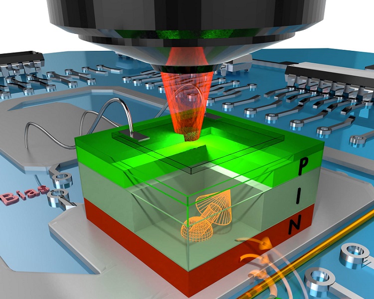
SiC quantum spintronics: towards quantum devices in a technological material
Theo Murphy international scientific meeting organised by Dr Cristian Bonato, Professor Joerg Wrachtrup and Dr Sang-Yun Lee.
Recent research has shown that spin-active colour centres in silicon carbide (SiC) are a promising system for quantum technology. In contrast to similar platforms, such as diamond, SiC is an industrially-mature material for micro-electronics, opening exciting prospects for integrated quantum devices. This symposium will interface leading academic and industrial researchers to discuss the potential of SiC-based quantum devices.
Recorded audio of the presentations will be available on this page within one month after the meeting has taken place.
Attending this event
This meeting has taken place.
Enquiries: contact the Scientific Programmes team
Organisers
Schedule
Chair
Dr Sang-Yun Lee, Korea Institute of Science and Technology, South Korea
Dr Sang-Yun Lee, Korea Institute of Science and Technology, South Korea
Sang-Yun Lee is currently a senior researcher at the Center for Quantum Information, Korea Institute of Science and Technology (KIST). He learned solid state physics, basic spectroscopy, and electron spin resonance during his MS, supervised by Professor Joo at the Korea University. For his PhD, he continued studying electron spin resonance and developed pulsed resonance techniques as a new spectroscopic tool on various defect states in semiconductors in Professor Boehme’s group at the University of Utah, USA. While he was working on spin qubits based on defects in solids in Professor Wrachtrup’s group at the University of Stuttgart, Germany, together with his colleagues, he successfully demonstrated quantum applications such as spin qubit creation and control, quantum magnetometry, and single photon sources based on isolated defects in silicon carbide. He and his colleagues are working together towards spin-to-photon interface in silicon carbide. Dr Lee has also settled in a new position in Korea to establish a research group working for quantum information using defects in wide-bandgap semiconductors.
| 09:00 - 09:10 | Welcome by the Royal Society and lead organiser |
|---|---|
| 09:10 - 09:40 |
Quantum spintronics with SiC defects

Professor Joerg Wrachtrup, University of Stuttgart, Germany
Professor Joerg Wrachtrup, University of Stuttgart, Germany |
| 09:40 - 09:55 | Discussion |
| 09:55 - 10:25 |
Coherent control of spin qudit modes associated with defects in SiC
Quantum bit or qubit is a two-level system, which builds the foundation for quantum computation, simulation, communication and sensing. Quantum states of higher dimension, ie, qutrits (D = 3) and especially qudits (D = 4 or higher), offer significant advantages. Particularly, they can provide noise-resistant quantum cryptography, simplify quantum logic and improve quantum metrology. Flying and solid-state qudits have been implemented on the basis of photonic chips and superconducting circuits, respectively. However, there is still a lack of room-temperature qudits with long coherence time and high spectral resolution. The silicon vacancy centers in silicon carbide (SiC) with spin S = 3/2 are quite promising in this respect. Here, Dr Astakhov reports a two-frequency protocol to excite and image multiple qudit modes in a SiC spin ensemble under ambient conditions. Strikingly, their spectral width is about one order of magnitude narrower than the inhomogeneous broadening of the corresponding spin resonance. By applying Ramsey interferometry to these spin qudits, a spectral selectivity of 600 kHz and a spectral resolution of 30 kHz are achieved. As a practical consequence, Dr Astakhov's team demonstrates absolute DC magnetometry insensitive to thermal noise and strain fluctuations. 
Professor Georgy Astakov, Institute of Ion Beam Physics and Materials Research, Germany
Professor Georgy Astakov, Institute of Ion Beam Physics and Materials Research, GermanyDr Georgy Astakhov received his PhD from the Ioffe Institute, Russia in 2000. He then worked at the Julius-Maximilians-University of Würzburg, Germany as a postdoctoral researcher, academic councilor and academic senior councilor. In 2017, Dr Astakhov obtained habilitation and served as a lecturer. Since 2018, Dr Astakhov is a senior scientist in the Institute of Ion Beam Physics Materials Research of the Helmholtz-Zentrum Dresden-Rossendorf, Germany and leads research group Quantum Materials and Technology. As a scientist, he investigates spin-related phenomena in semiconductor nanostructures and magnetic semiconductors using various polarization-sensitive spatiotemporal spectroscopies in the visible, infrared and terahertz spectral ranges. His current interests encompass spin defects for quantum applications and topological states of matter. |
| 10:25 - 10:40 | Discussion |
| 10:40 - 11:00 | Coffee |
| 11:00 - 11:30 |
Optical Properties of Single Silicon Vacancies in 4H-SiC
Defects in wide bandgap materials have generated substantial interest as promising systems for quantum information and quantum sensing. SiC is an attractive material in terms of mature growth and fabrication technology and also has a low natural abundance of nuclear spins, which reduces spin dephasing. One promising defect system is the silicon monovacancy in SiC (VSi), which has a spin-3/2 ground state that can be optically polarized and maintain long spin coherence times even at room temperature. While significant work has been performed to study the spin properties of VSi for ensembles and even single defects, the optical properties and their connection to the spin system are less developed. In this presentation, Dr Samuel Carter will report on optical spectroscopy of single VSi defects, primarily V2 defects, at low temperatures. Using laser excitation spectroscopy, the zero phonon line (ZPL) transitions corresponding to the m_s=±1⁄2 and m_s=±3⁄2 spin states are resolved, with a linewidth down to 70 MHz. The spin polarization dynamics are measured for resonant and non-resonant optical excitation, and the results agree well with a theoretical model of the spin states and intersystem crossing. These results are essential to understanding the optical and spin physics of the defect and for developing a spin-photon interface. Dr Carter will also discuss results on producing VSi at precise locations using ion implantation and efforts to fabricate photonic crystal cavities to enhance defect emission. This work was supported by the Office of Naval Research and the Office of the Secretary of Defense Quantum Sciences and Engineering Program. 
Dr Samuel G Carter, US Naval Research Laboratory, USA
Dr Samuel G Carter, US Naval Research Laboratory, USADr Samuel G Carter is an experimentalist in the area of condensed matter physics with interests in optically active quantum dots, defect spins in solids, ultrafast optical control, and quantum information science. He received his PhD in Physics in 2004 at the University of California, Santa Barbara, working with Professor Mark Sherwin on terahertz-driven quantum wells. After postdoctoral studies at NIST and the University of Colorado, Boulder with Professor Steve Cundiff on ultrafast optical spectroscopy of semiconductors, he joined the Naval Research Laboratory in Washington, DC in 2007. There he works in the Electronics Science and Technology Division on developing solid state implementations for quantum information science and technology. |
| 11:30 - 11:45 | Discussion |
| 11:45 - 12:15 |
Quantum control of spins in silicon carbide with photons and phonons
There is a growing interest in exploiting the quantum properties of electronic and nuclear spins for the manipulation and storage of quantum information. Here Professor Awschalom and his team focus on recent developments in controlling and connecting spins in silicon carbide (SiC) using photons and phonons. They find that defect-based electronic states in SiC can be isolated and optically probed at the single spin level with surprisingly long spin coherence times and high-fidelity control within a wafer-scale material operating at near-telecom wavelengths. Moreover, a detailed study of the defect spin-photon interface yields efficient quantum control in various polytypes along with near-unity electronic and nuclear polarization, highlighting the potential of SiC for photon-mediated entanglement. In addition, they use Gaussian surface acoustic wave (SAW) resonators to exploit both the piezoelectric and isotropic phonon properties of SiC to create Autler-Townes splittings, mechanically drive coherent Rabi oscillations, and explore spin-strain coupling contributions from all mechanical degrees of freedom, including shear. The spatial confinement of phonons is mapped using a nanoscale diffraction imaging technique with a synchrotron to focus x-rays and provide 25 nm spatial resolution. This work expands the versatility of optically and mechanically driven spins in a material with developed device and fabrication capabilities, and shows promise towards integrating quantum states with nanomechanical systems for both control and communication.
Professor David Awschalom, University of Chicago, USA
Professor David Awschalom, University of Chicago, USADavid Awschalom received his PhD in physics from Cornell University, and was a research staff member and manager at IBM Research. Professor Awschalom joined the University of California-Santa Barbara as a Professor of Physics, Electrical and Computer Engineering serving as the Peter J Clarke Professor and Director of the California NanoSystems Institute. He is currently the Liew Family Professor of Spintronics and Quantum Information and Deputy Director in the Institute for Molecular Engineering at the University of Chicago, and senior scientist at Argonne National Laboratory. He works in the fields of spintronics and quantum information engineering, developing methods to investigate the quantum states of individual electrons, nuclei, and photons in the solid state. Professor Awschalom received the Oliver E Buckley Prize and Julius Edgar Lilienfeld Prize, the Europhysics Prize, the David Turnbull Award, the Newcomb Cleveland Prize, and the International Magnetism Prize. He is a member of the American Academy of Arts & Sciences, the National Academy of Sciences, the National Academy of Engineering, and the European Academy of Sciences. |
| 12:15 - 12:30 | Discussion |
| 12:30 - 13:30 | Lunch |
Chair
Dr Cristian Bonato, Heriot-Watt University, UK
Dr Cristian Bonato, Heriot-Watt University, UK
Cristian Bonato is Assistant Professor at Heriot-Watt University. He holds a Degree in Physics (2004) and a PhD in Electrical Engineering (2008), both from the University of Padova, Italy. Before joining Heriot-Watt University he held post-doctoral positions at Leiden University and at the Technical University of Delft, both in the Netherlands, where he investigated cavity quantum electrodynamics and spin control in III-V semiconductors and diamond. His research focuses on the development of spin-based quantum technology in different material platforms, for applications to sensing and communication
| 13:30 - 14:00 |
Integrated optics in silicon carbide
The excellent physical properties of silicon carbide offer a wide range of potential applications for optics, from photonic devices spanning a wide wavelength range to non-linear and quantum optics. This talk will discuss the recent advances on the integration of optical components in silicon carbide, particularly focusing on the 3C polytype. A complete photonic platform that includes grating couplers, waveguides and ring resonators has been developed, offering a platform for classical and non-linear optics. The demonstration of photonic crystal cavities that show high field confinement will be presented. Their integration with colour centres can expand applications to the quantum technology domain. Finally, the extension to longer wavelength ranges will be discussed. Sub-wavelength confined cavities and strong nonlinearities can be achieved in the mid-infrared band by harnessing the unique phononic properties of SiC. 
Dr Alberto Politi, University of Southampton, UK
Dr Alberto Politi, University of Southampton, UKAlberto Politi received his PhD degree at the Centre for Quantum Photonics, University of Bristol, UK in 2010 where he demonstrated the first chip for quantum photonics, the first integrated optical quantum algorithm and other key ingredients for optical quantum technologies. After a postdoctoral position at the Center for Quantum Photonics, he was research assistant at the University of California, Santa Barbara, USA from 2011-2013 working on solid-state quantum computing using silicon carbide colour centres. From 2013 Alberto is Lecturer in the School of Physics and Astronomy at Southampton, where he leads the Quantum nano-Photonics group. |
|---|---|
| 14:00 - 14:15 | Discussion |
| 14:15 - 14:45 |
Optimizing Spin and Optical Defect Signatures in SiC Nanocavities
Various polytypes of SiC have demonstrated spin-active point defects with substantial coherent times at room temperature. A single defect, such as the silicon vacancy (SiV) in 4H SiC, occupying different lattice sites (hexagonal or cubic) will produce different zero-phonon-line (ZPL) emission wavelengths. Thus, there is a richness of information about these defects relating details of the local atomic environment, such as strain, to the spin- and photon-dependent performance of the defects. High quality SiC nanocavities, designed and fabricated to match the embedded defects, not only enhance the optical emission of these defects, but also serve as “nanoscopes” that can elucidate details of the defects’ atomic environment. This talk will illustrate the application of nanobeam photonic crystal cavities, fabricated from 4H-SiC, to achieve an 80-fold optical enhancement of a Si-vacancy transition with emission at about 860 nanometers. The cavities can also highlight details of defect motion at elevated temperatures and suggest avenues of better placement of defects within the cavities. 
Professor Evelyn Hu, Harvard University, USA
Professor Evelyn Hu, Harvard University, USAEvelyn Hu is the Tarr-Coyne Professor of Applied Physics and Electrical Engineering at the John A. Paulson School of Engineering and Applied Sciences at Harvard. Prior to Harvard, she was a faculty member at UCSB, in the Departments of Materials, and of Electrical and Computer Engineering. While at UCSB, she also served as the founding Scientific co-Director of the California NanoSystems Institute, a joint initiative between UCSB and UCLA. Before joining UCSB, she worked at Bell Labs in both Holmdel and Murray Hill. She is a member of the National Academy of Sciences, the National Academy of Engineering, the American Academy of Arts and Sciences, and the Academica Sinica of Taiwan. She is a recipient of an NSF Distinguished Teaching Fellow award, an AAAS Lifetime Mentor Award, and holds honorary Doctorates from the University of Glasgow, Heriot-Watt University, Hong Kong University of Science and Technology, and the University of Notre Dame. |
| 14:45 - 15:00 | Discussion |
| 15:00 - 15:30 |
Tea
|
| 15:30 - 16:00 |
Silicon carbide color center photonics
Silicon carbide color centers are promising systems for quantum communication, spintronics and sensing. Their integration with photonic devices is a path to scalability, higher efficiency and new regimes of operation. Advanced material processing is the main challenge in the realization of the designed devices. So far, high quality color centers have been available only in bulk substrates, which impedes the development of freestanding nanophotonic structures, such as photonic crystal cavities. This talk will report on the progress in the development of nanofabrication processes in bulk silicon carbide, and hybrid silicon carbide-diamond platform, where color centers are hosted in nanodiamonds. The realized systems provide a scalable interface for addressing individual SiC color centers and demonstrate SiC-assisted Purcell enhancement of diamond color center emission. Furthermore, theoretical insights into cavity quantum electrodynamics of color centers will be discussed. The small inhomogeneous broadening of color center ensembles is leveraged to potentially achieve collective coupling to a common cavity. Such regime not only exhibits arbitrarily high light-matter interaction, but also holds novel quantum light generating mechanisms. In addition to the conventional photon blockade that results in a steam of individual photons, multi-emitter-cavity systems can facilitate the so-called subradiant photon blockade with higher purity of single-photons. Finally, they also offer three-photon generating channels. 
Dr Marina Radulaski, Stanford University, USA
Dr Marina Radulaski, Stanford University, USAMarina Radulaski is a Nano- and Quantum Science and Engineering Postdoctoral Fellow at Stanford University’s Ginzton Laboratory, and an incoming Assistant Professor of Electrical and Computer Engineering at the University of California at Davis. She obtained a PhD in Applied Physics from Stanford University under the supervision of Professor Jelena Vuckovic, a BSc/MSc in Physics from the University of Belgrade, Serbia, and a BSc/MSc in Computer Science from the Union University, Serbia. Marina was selected among the Rising Stars in EECS in 2017, Stanford Graduate Fellows 2012-2014, and Scientific American’s “30-Under-30 Up and Coming Physicists” in 2012. She has performed research internationally at Berkeley Lab, Hewlett-Packard Labs, Oxford University, IQOQI Vienna, Helmholtz Center Berlin, and more. |
| 16:00 - 16:15 | Discussion |
| 16:15 - 16:45 |
High-performance microcavity arrays for solid-state qubits
Numerous applications in quantum technology, including photon generation, nanoparticle manipulation, and optical readout of qubits, require enhanced interactions between light and matter. Such an enhancement can be achieved with the use of microcavities, in which strong spatial confinement and high-reflectivity mirrors can drastically increase the desired interaction strength. For several of the intended applications, such as quantum computation and communication, it will furthermore be beneficial to create large numbers of efficient light-matter interfaces. In this presentation, results from the University of Vienna in creating high-performance microcavity arrays will be discussed. The microcavities are micro-machined using highly precise lithographic methods, which enable the creation of large arrays of devices. By tailored optimization of the mirror morphology and surface quality, these microcavities have now reached a mirror reflectivity which approaches that of the best available macroscopic substrates. Lithographically defined alignment structures were furthermore used to robustly align arrays of micromirrors to each other while preserving their high performance values. As each microcavity needs to resonant with the desired optical transition, tuning of the microcavities using integrated micro-electromechanical actuators will also be described. Finally, efforts towards the integration of optically active defects in diamond and silicon carbide will be presented. 
Dr Michael Trupke, University of Vienna, Austria
Dr Michael Trupke, University of Vienna, AustriaMichael Trupke is a researcher with core interests in quantum technology, quantum optics and solid state physics. In his PhD studies and postdoctoral work at Imperial College, London, he developed techniques and micro-machined devices for the detection and manipulation of ultracold atoms. Following this work he became team leader at TU Wien, where he built laboratories for the study of diamond defects at room temperature and under cryogenic conditions. In 2016 he accepted a position at the University of Vienna. His team is active in the study of point defects in large-bandgap semiconductor crystals for quantum sensing and information technology, and in the use of micro-technology for applications in quantum science. |
| 16:45 - 17:00 | Discussion |
Chair
Dr Marina Radulaski, Stanford University, USA
Dr Marina Radulaski, Stanford University, USA
Marina Radulaski is a Nano- and Quantum Science and Engineering Postdoctoral Fellow at Stanford University’s Ginzton Laboratory, and an incoming Assistant Professor of Electrical and Computer Engineering at the University of California at Davis. She obtained a PhD in Applied Physics from Stanford University under the supervision of Professor Jelena Vuckovic, a BSc/MSc in Physics from the University of Belgrade, Serbia, and a BSc/MSc in Computer Science from the Union University, Serbia. Marina was selected among the Rising Stars in EECS in 2017, Stanford Graduate Fellows 2012-2014, and Scientific American’s “30-Under-30 Up and Coming Physicists” in 2012. She has performed research internationally at Berkeley Lab, Hewlett-Packard Labs, Oxford University, IQOQI Vienna, Helmholtz Center Berlin, and more.
| 09:00 - 09:30 |
Intrinsic defects in silicon carbide: engineering and charge state control
Silicon carbide (SiC) has recently shown to be a promising material that hosts colour centers with excellent optical and spin properties suitable for different applications in quantum technology. Among these, intrinsic defects, such as the Si vacancy and the divacancy, can be created irradiation of high-energy particles with well-controlled concentrations down to the levels that allow to isolate single emitters. However, controlling their charge states for achieving bright and stable single emitters is still a challenge. This requires controlling the charge compensation processes between residual impurities, such as the shallow N donor and shallow acceptors (Al and B), and other intrinsic defects induced by irradiation in order to tune the Fermi level. In this talk, an overview on defects created by electron irradiation in SiC and charge compensation processes in irradiated low-doped and undoped n-type and p-type epitaxial layers grown by chemical vapour deposition and commercial high-purity semi-insulating materials is given. Based on the data from electron paramagnetic resonance, deep level transient spectroscopy, photoluminescence and theoretical calculations, the charge state control of the Si vacancy and the divacancy and the role of the carbon vacancy in tuning the Fermi level are discussed. 
Professor Nguyen Tien Son, Linköping University, Sweden
Professor Nguyen Tien Son, Linköping University, SwedenNguyen Tien Son received the BSc degree in Physics from the Vietnam National University (VNU), Hanoi, Vietnam in 1979. After graduation, he started his academic career as an assistant lecturer and lecturer at Department of Physics, VNU, Hanoi. During 1987-1988 and 1991-1993, he joined the group of Semiconductor materials at the Van der Waals-Zeeman Institute, University of Amsterdam (UvA), The Netherlands, as a Ph.D. student and worked on magnetic resonance of point defects in semiconductors. He received the Ph.D. degree in 1993 at UvA. Since then he has worked at the Department of Physics, Chemistry and Biology (IFM), Linköping University (LiU), Sweden. He is currently a Professor at IFM, LiU. His main research activity includes investigation of fundamental properties and defect physics of semiconductors, such as SiC, III-nitrides, ZnO, Ga2O3, and MoS2, using magnetic resonance, optical and electrical characterizations. In recent years, his research focuses on defect spins in SiC for applications in quantum technology. |
|---|---|
| 09:30 - 09:45 | Discussion |
| 09:45 - 10:15 |
Identification and tunable optical coherent control of transition-metal spins in silicon carbide
Colour centers in wide-bandgap semiconductors are attractive systems for quantum technologies since they can combine long-coherent electronic spin and bright optical properties. Several suitable centers have been identified, most famously the nitrogen-vacancy defect in diamond. However, integration in communication technology is hindered by the fact that their optical transitions lie outside telecom wavelength bands. Several transition-metal impurities in silicon carbide do emit at and near telecom wavelengths, but knowledge about their spin and optical properties is incomplete. We present all-optical identification and coherent control of molybdenum-impurity spins in silicon carbide with transitions at near-infrared wavelengths. Our results identify spin S=1/2 for both the electronic ground and excited state, with highly anisotropic spin properties that we apply for implementing optical control of ground-state spin coherence. Our results show optical lifetimes of about 60 ns and inhomogeneous spin dephasing times of about 1 microsecond, establishing relevance for quantum spin-photon interfacing. 
Professor Caspar H van der Wal, University of Groningen, The Netherlands
Professor Caspar H van der Wal, University of Groningen, The NetherlandsCaspar H van der Wal obtained his PhD degree in 2001, with Professor Hans Mooij at Delft University of Technology for research on quantum coherent dynamics of superconducting circuits. He is currently full professor in Physics of Quantum Devices at the Zernike Institute for Advanced Materials in Groningen. His research focuses on exploring spintronic and quantum information functionalities with electron spins and nuclear spins in semiconductor devices, using quantum optical methods and electron transport methods. He won an NWO-VIDI Grant (2005) and an ERC Starting Grant (2011). As of 2016 he is scientific director of the Zernike Institute for Advanced Materials. |
| 10:15 - 10:30 | Discussion |
| 10:30 - 11:00 | Coffee |
| 11:00 - 11:30 |
Ab initio study of SiC qubits for hyperpolarization, quantum sensing and communication
Paramagnetic and luminescent point defects in silicon carbide (SiC) are very promising for integrating semiconductor technology and quantum technology into a single platform. In particular, divacancy defects akin to nitrogen-vacancy center in diamond show similar electronic structure but the former are more sensitive to strain and electric fields that enables to employ them for quantum sensing protocols. First principles calculations show that divacancies in SiC can be also used to polarize the surrounding nuclear spins at arbitrary direction by controlling a small, constant magnetic field. First principles calculations also revealed interesting features on the silicon-vacancy quantum bits. Silicon-vacancy quantum bits have a special electronic structure that makes the optical emission almost intact to electrical stray fields and makes it a prominent candidate for quantum communication in the near infrared region with conversion to the telecom wavelengths. Finally, a transition metal defect will be discussed, vanadium, that was originally used to compensate electrically active impurities in SiC. Vanadium has optical transition in the O-band of telecom communication and an electron spin that can be detected by traditional electron spin resonance techniques which implies favourable spin coherence times. First principles calculations indicate that the Debye-Waller factor of the optical transition is around 0.5 that makes this centre a promising candidate for quantum communication in the telecom wavelengths applied in the every-day classical communication. 
Professor Adam Gali, Hungarian Academy of Sciences, Hungary
Professor Adam Gali, Hungarian Academy of Sciences, HungaryAdam Gali is a chief scientific advisor in Wigner Research Centre, the leader of “Lendület” Semiconductor Research Group, founder of Wigner Advanced Materials Integrated Laboratory (ADMIL) and Optically Detected Magnetic Resonance Laboratory for Quantum Technology, an associate professor at Budapest University of Technology and Economics, Doctor of Science of the Hungarian Academy of Sciences. He studies the magneto-optical properties of point defects in semiconductors and semiconductor nanostructures by means of ab initio methods and experimental techniques, to develop efficient biomarkers, solar cells and solid state defect quantum bits. He recently has developed and implemented methods to fully characterize nitrogen-vacancy centre in diamond from first principles methods that can be applied to other solid state defect quantum bits such as divacancy in silicon carbide and other defects in three- and two-dimensional solids. |
| 11:30 - 11:45 | Discussion |
| 11:45 - 12:15 |
Defects in SiC: Electronic structure, spin control, and spin-photon interfaces
Colour center defects in solids are attractive candidates for quantum information processing. Silicon carbide (SiC) has emerged as a technologically viable material for quantum technologies. It hosts defects that can be exploited both for spin-based and photonics applications. I will present our work on the electronic structure of the silicon vacancy defect in SiC and the intersystem crossing mechanism under optical drive. These results enable the design of spin-photon interfaces that can be used to generate highly entangled ‘graph’ states of photons, which are crucial for applications in quantum computation and communication. Abstract and presentation provided by Professor Sophia Economou, Virginia Tech, USA 
Wenzheng Dong, PhD candidate, Virginia Tech, USA
Wenzheng Dong, PhD candidate, Virginia Tech, USAWenzheng Dong is a fourth year PhD candidate in Physics Department at Virginia Tech. He is advised by Professor Sophia Economou since 2016. His research focuses on theoretical condensed matter physics, especially on application of silicon carbide defect in quantum information science. |
| 12:15 - 12:30 | Discussion |
| 12:30 - 13:30 | Lunch |
Chair
Professor Joerg Wrachtrup, University of Stuttgart, Germany
Professor Joerg Wrachtrup, University of Stuttgart, Germany
| 13:30 - 14:00 |
Laser fabrication of colour centres in silicon carbide and diamond
Optically active colour centres in silicon carbide and diamond have attracted considerable attention in the past few years as candidates for quantum applications, single photon sources, nanomagnetic resonance imaging and spintronics devices. The control of defects position and their placement at a desired location in a chip, necessary to integrate them within optical and electronic devices, is still a challenge. Recently, laser writing emerged as a new tool to generate vacancies in crystals as a starting point for the formation of colour centres. In this work, a laser writing method has been used to produce colour centres in 4H and 6H bulk silicon carbide and diamond by using a femtosecond laser with repetition rate of 200kHz. Array of colour centres were fabricated by different pulse laser energies in sites of square grids at varied depths (from surface level to 10µm below surface). We optically characterized the fabricated colour centres using confocal imaging and spectroscopy. We show that the technique can produce specifically the silicon vacancy colour centres with a relevant emission in the 900nm and other emitters in the visible range. This method can be adopted to engineer colour centres in silicon carbide for the above-mentioned applications in addition to display fabrication and light emitting diodes. 
Professor Stefania Castelletto, RMIT University, Australia
Professor Stefania Castelletto, RMIT University, AustraliaStefania Castelletto is currently associate professor in the School of Engineering at the Royal Melbourne Institute of Technology University in Melbourne, Australia and holds a Dottorato di Ricerca (PhD equivalent) from the School of Engineering at the Polytechnic of Turin, Italy. Before this appointment she covered various research positions as Senior Fellow at the following Australian universities; Macquarie University, Swinburne University of Technology and The University of Melbourne. She was part of an Australian Research Council Centre of Excellence for engineered quantum systems. Before she was group leader at the Italian National Metrology Research Centre and responsible for the research and development of quantum technologies based on non-classical states of light, such as quantum cryptography and quantum imaging. She has been visiting scientist at the National Institute of Technology and Standards for two years. Her recent focus on research is on colour centres in diamond and silicon carbide for applications in quantum sensing, single photon sources and super-resolution imaging. |
|---|---|
| 14:00 - 14:15 | Discussion |
| 14:15 - 14:45 |
CVD growth of ultra-high purity SiC: Challenges and solutions
Epitaxial growth is required to obtain high quality and high purity layers of 4H-SiC with controlled doping concentration. Such layers are usually grown using horizontal hot-wall CVD reactor, developed at Linköping university in 90’s, which today is a standard reactor design being used worldwide. Off-cut substrates are used to replicate substrate’s polytype in the epilayer and smooth surface. High quality large area (150 mm diameter) substrates are commercially available and off-cut epitaxial growth is already mastered to produce thick layers suitable for electronic devices. However, epitaxial growth process is not matured enough to produce ultra-high purity epilayers with extremely low doping and complex layer structure with controlled n- and p-type doping which is one of the basic requirements for spintronics applications. This is mainly due to high temperature growth (>1600 C) which leads to the formation of high density intrinsic defects and also limits the control over residual doping and surface morphology. At Linköping University, Dr Ul-Hassan has unique possibility to grow epilayers at extremely fast growth rate (>100 m/h) which enables significantly low background doping, growth of isotopically enriched 4H-28Si12C epilayers with high thermal conductivity and no nuclear spin, and growth on on-axis substrates which leads to ultra-high purity and low defect density epilayers. In this talk, Dr Ul-Hassan will present the current status of SiC epitaxial growth and discuss different challenges and possible solutions to obtain ultra-high purity epilayers with controlled low doping using standard and non-standard growth processes on different off-cut substrates. 
Dr Jawad Ul-Hassan, Linköping University, Sweden
Dr Jawad Ul-Hassan, Linköping University, SwedenJawad Ul-Hassan received MSc Physics (1998) from University of the Punjab, Lahore, Pakistan, and M.S. Material Physics and Nanotechnology (2003) and PhD in Semiconductor Physics (2009) from Linköping University, Linköping, Sweden. In 2011 he joined Linköping University and currently he is working as Associate professor in the Semiconductor Materials group. He is responsible for epitaxial growth of SiC and graphene on SiC and leading the development of these materials for high power/high frequency electronic devices and biomedical applications in several projects. He has authored or co-authored over 90 publications. |
| 14:45 - 15:00 | Discussion |
| 15:00 - 15:30 | Tea |
| 15:30 - 16:00 |
Perspective on Silicon Carbide Devices: flavours, defects and processing
A revolution in power electronics is being brought about by the maturity of Silicon Carbide (SiC) as a wide bandgap semiconductor, which has been forecast to dominate the high voltage power electronics market by 2022. SiC possesses attractive qualities in addition to its high electric breakdown field, which allow it to be a material for high frequency, harsh environment and high temperature applications. When compared to Silicon, SiC power devices allow higher voltage and higher temperature operation at greatly improved efficiency. SiC is the key to future power electronics for voltages above 600 V where Silicon undergoes severe efficiency degradation resulting in significant power losses. HVDC conversion requires bipolar transistors and diodes, PiN, BJT, GTO or IGBT devices, however, SiC unipolar SBDs and MOSFETs have already been commercialised as discrete devices and incorporated in inverter modules and so are an early indicator and true litmus test in the trend of future SiC technology. The use of SiC in Quantum applications can benefit from this massive body of work which is still progressing at an incredible pace. The different flavours of power device will be discussed in addition to how the material quality can affect the device performance. Best practices, conventional wisdoms and unknowns in the difficulty of processing such devices will also be touched on. 
Dr Vishal Shah, University of Warwick, UK
Dr Vishal Shah, University of Warwick, UKDr Shah has over 10 years’ experience in developing materials for use in new and developing technologies. His research interests are driven by improving semiconductor materials and devices, having completed a PhD in physics at Warwick in 2009. He has published 26 journal papers, 26 conference papers, 4 book chapters and made over 50 conference contributions, equating to a h-index of 12 and a total of 327 citations as of Jan 2018. He has filed 2 patents on past work and is used to exploring the commercial applications and implications of research. His research at the School of Engineering at Warwick develops solid-state technology for numerous application areas: power distribution, energy production, thermoelectrics, photovoltaics, micro-electronics/CMOS, µ-electromechanical systems (MEMS), sensing technologies and quantum technology. |
| 16:00 - 16:15 | Discussion |
| 16:15 - 16:45 |
Growth of silicon carbide for new applications
The growth of silicon carbide crystals is today made with three different technologies: sublimation, HTCVD and liquid phase. Sublimation is the dominating process and it produce high quality n-type conducting substrates. CVD is used for epitaxial growth and can be both n-type and p-type doped depending on need. The key properties in the n-type substrates is developed and specified to fit power device (diodes and transistors) application and for the semi-insulating substrates it is to fit for nitride epitaxy targeting high frequency HEMT devices. For applications in the quantum spintronics field it is new requirements on the substrate and the epitaxy. The talk will describe the different methods for growth of crystals and epitaxy together with the benefit or disadvantage they have for applications in the quantum spintronics. The possibility of post-growth processing to change the properties of the substrates and epitaxy will also be discussed. 
Dr Björn Magnussonk, Norstel AB, Sweden
Dr Björn Magnussonk, Norstel AB, SwedenWith 20 years’ experience of silicon carbide (SiC) Björn Magnusson has in depth knowledge and hands-on experience in crystal growth, wafering, characterization and epitaxy. Most of his research is made at Linköping University and the industrial experience is from Okmetic and Norstel. The work has resulted in processes, products, granted patents and more than 70 scientific journal and conference publications. Dr Magnusson is currently responsible for the production at Norstel. He supervises and has an active role in all parts of our activities, all the way from machine and process to customer. |
| 16:45 - 17:00 |
Chair's closing summary
Professor Joerg Wrachtrup, University of Stuttgart, Germany
Professor Joerg Wrachtrup, University of Stuttgart, Germany |